DIY SMD PCB Assembly: Tools and Organization for Hobbyists
Posted on May 24, 2025 • 14 min read • 2,965 words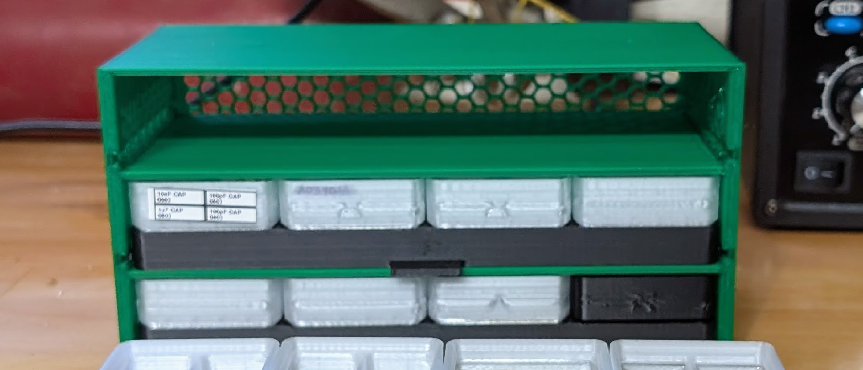
Challenges of Hobbyist PCB Assembly
I design hobbyist-level printed circuit boards (PCBs1) for personal and home use. I order the boards themselves from vendors such as PCBWay (who sponsored this post). I’ve never made enough of any particular kind of device to try ordering the boards from these vendors pre-assembled, with all the components in-place. So I have always done the assembly of these boards myself.
When I started:
- Board assembly took me a very long time.
- My boards often did not work upon initial assembly. They sometimes required debug and fixing before they worked properly.
- Buying components could be (relatively) expensive.
This post presents a few tricks I’ve learned to make things work better. These are things I would have liked to have known when I started, so maybe they will be useful to you. Some readers likely know much better methods. Either way, I’d like to know, so please add a comment below!
Improvements I’ve made include:
- Component storage and preparation for assembly:
I found some storage solutions online and designed some of my own, which help manage SMD
components.
These can all be made using a 3D-printer.
My designs and selection integrate with the Gridfinity2 storage system.
- Custom pick-bins for SMD3 components, and
- A cabinet designed for storing these components in bins.
- Bulk-storage bins for SMD components.
- Component-tape dispensers (found online).
- Assembly tricks:
- Using component labels on PCB boards that encode both the component type and value for capacitors and resistors with the values I use the most often.
- Use of the pick-bins and component-tape dispensers for getting components close to the board at assembly time and simplifying pick-and-place.
- A solder paste and soldering method that reliably produces working boards.
- Component purchase and tracking:
- Building an inventory database.
- Learning which components to buy in bulk from AliExpress (and sometimes Amazon).
This post is a dense overview of a bunch of projects and methods. Let me know if it would be useful to go into more depth about any in particular.
The OpenSCAD source files for my designs that are described in this post are published at my SMD-Gridfinity GitHub repository.
The Challenge of SMD Assembly
Hand-assembling boards with surface-mount components can take a long time, particularly because
dealing with the tiny components is awkward.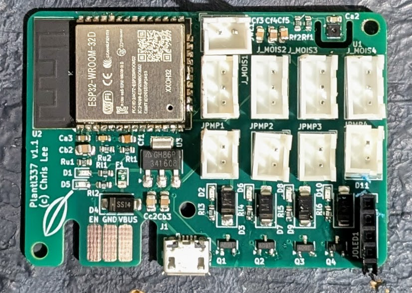
In my post on assembling Dough133, I discussed some things I have learned about assembling PCBAs. The summary is:
- Order a stencil with PCB boards from board vendors, and:
- Add screw-holes in the corner of the stencils, by making sure the drill hole is in the solder-paste Gerber file that is sent to the board manufacturer. This allows you to hold the stencil exactly in place with screws when applying solder paste to your PCB. (Update: I found a better way to hold the stencil in place! Please see Holding stencils in place for PCB soldering).
- Order a custom-sized stencil that will fit in the same box as the boards. This can dramatically reduce shipping costs. I order a size that allows a 1cm border around the board.
- A lead-free solder paste (183°C melting point) from from AliExpress has worked well for me.
- I use a cheap T-962A reflow oven with some modifications hobbyists often use to improve its performance (and so that its thermal insulation doesn’t catch fire!).
As discussed in that post, the start of the assembly is:
- Screw the PCB onto the solder-paste stencil.
- Use a solder paste syringe to deposit paste around the holes in the stencil, then use a putty knife to make sure all holes in the stencil are filled.
- Unscrew the stencil from the board, then clean the stencil with alcohol and a Q-tip to avoid solder paste hardening in the stencil holes between uses.
- Place the PCB in clamps under a microscope, to prepare for assembly.
- Pick components out of the SMD component tapes to populate the board.
Since that post, I’ve worked on making the process of populating the board less of a burden.
Typically, components like resistors, capacitors, transistors, and small integrated circuits are packaged in linear “tape.” This packaging is designed for robotic pick-and-place systems.
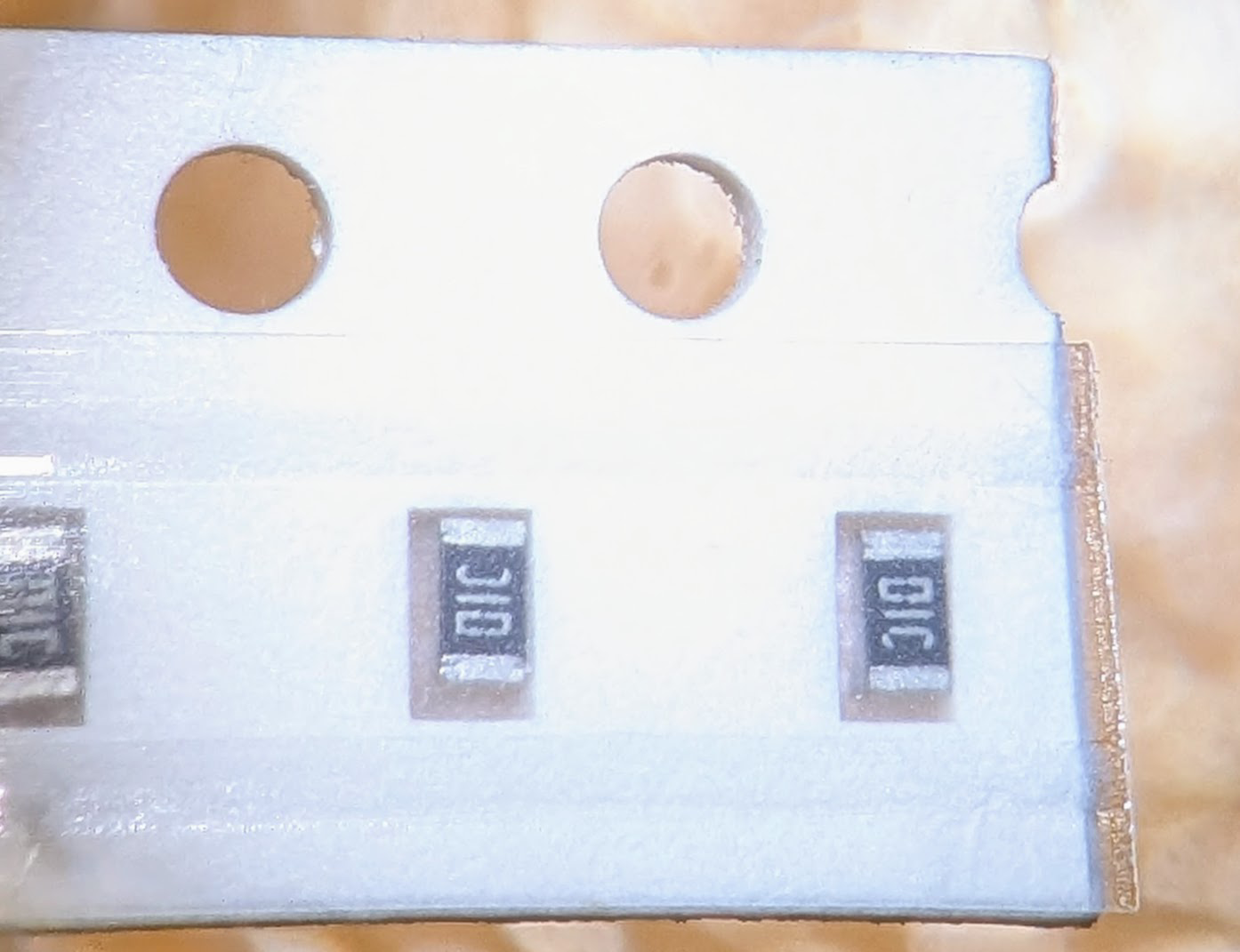
It can be awkward to use tweezers to expose the components and grasp them.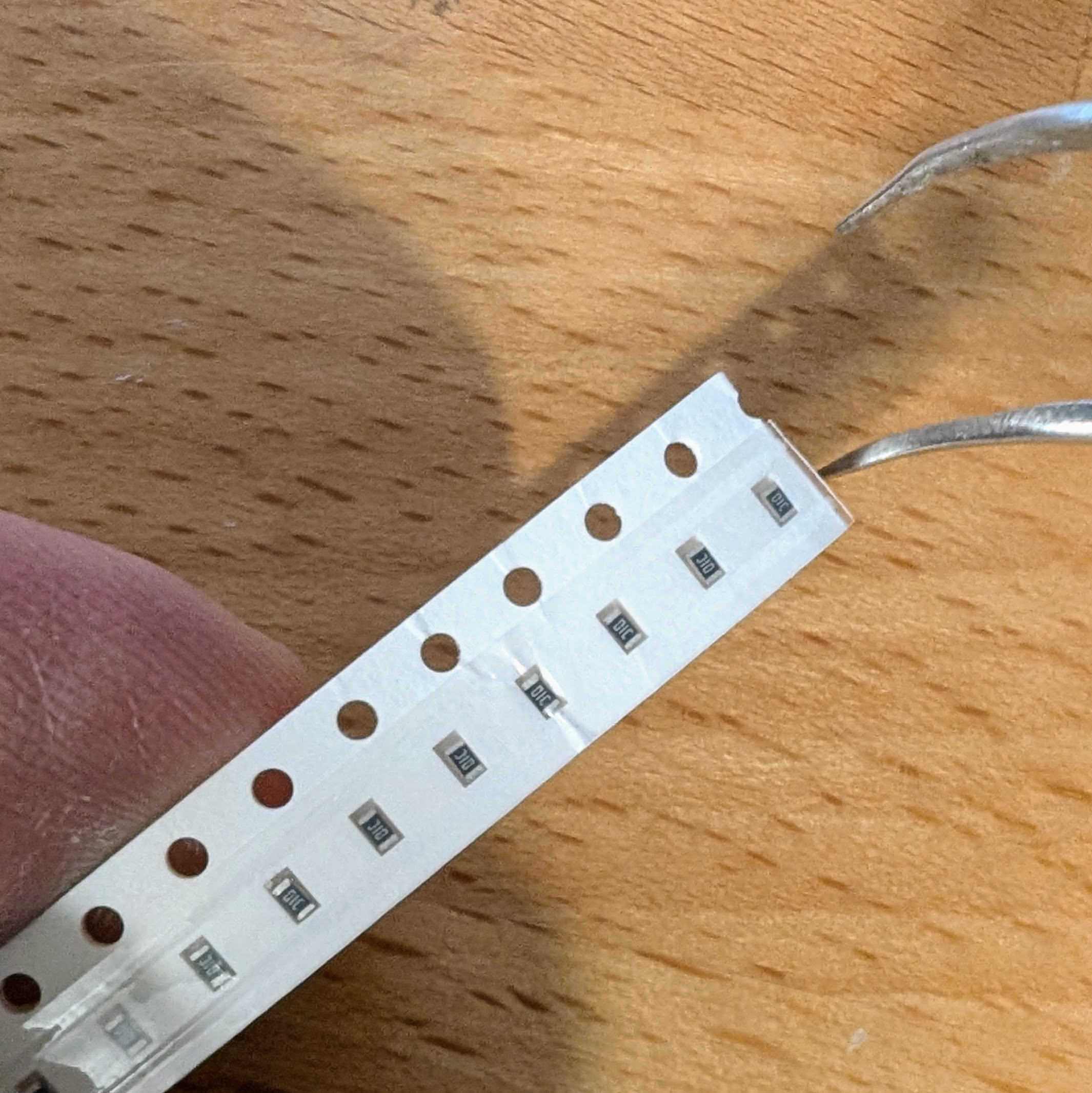
When I made my first few boards, I was using a printed spreadsheet of components (a BOM4) and an enlarged printed map of the board, both generated with KiCAD5, to figure out which component to place in each location of the PCB. I determined the next component I wanted to place from the map and BOM, found the carrier tape in my storage compartments that held the component I wanted, used tweezers to remove the component from the tape and let it fall onto the board, then picked-up the component with tweezers and moved it to its proper position on the board. This took forever, and a I spent a fair amount of time searching for tiny components which bounced off the board and ended-up somewhere on my workbench.
After a couple iterations, I built a system which works much better for me. It greatly speeds assembly by making it easier to:
- Remove components from tape and not lose components.
- Get the right components to the place the board will be assembled.
- Figure out which component to place without referring to BOMs and diagrams.
- Pick up components with tweezers.
Ordering PCBs from Manufacturers
In response to the first post on my Plant133 project, PCBWay reached out and asked me to try their PCB prototyping service. I ordered a set of my Room133 boards from PCBWay and they came out great – much thanks to PCBWay for helping a simple blog with “selective appeal”!
I generate Gerber files from KiCAD, upload to the vendor web site, select lead-free finish, order stencils if needed (see above about sizing these), and choose shipping to weigh price against my impatience. Shipping can easily be as much as board production, so it is best to batch up orders if possible.
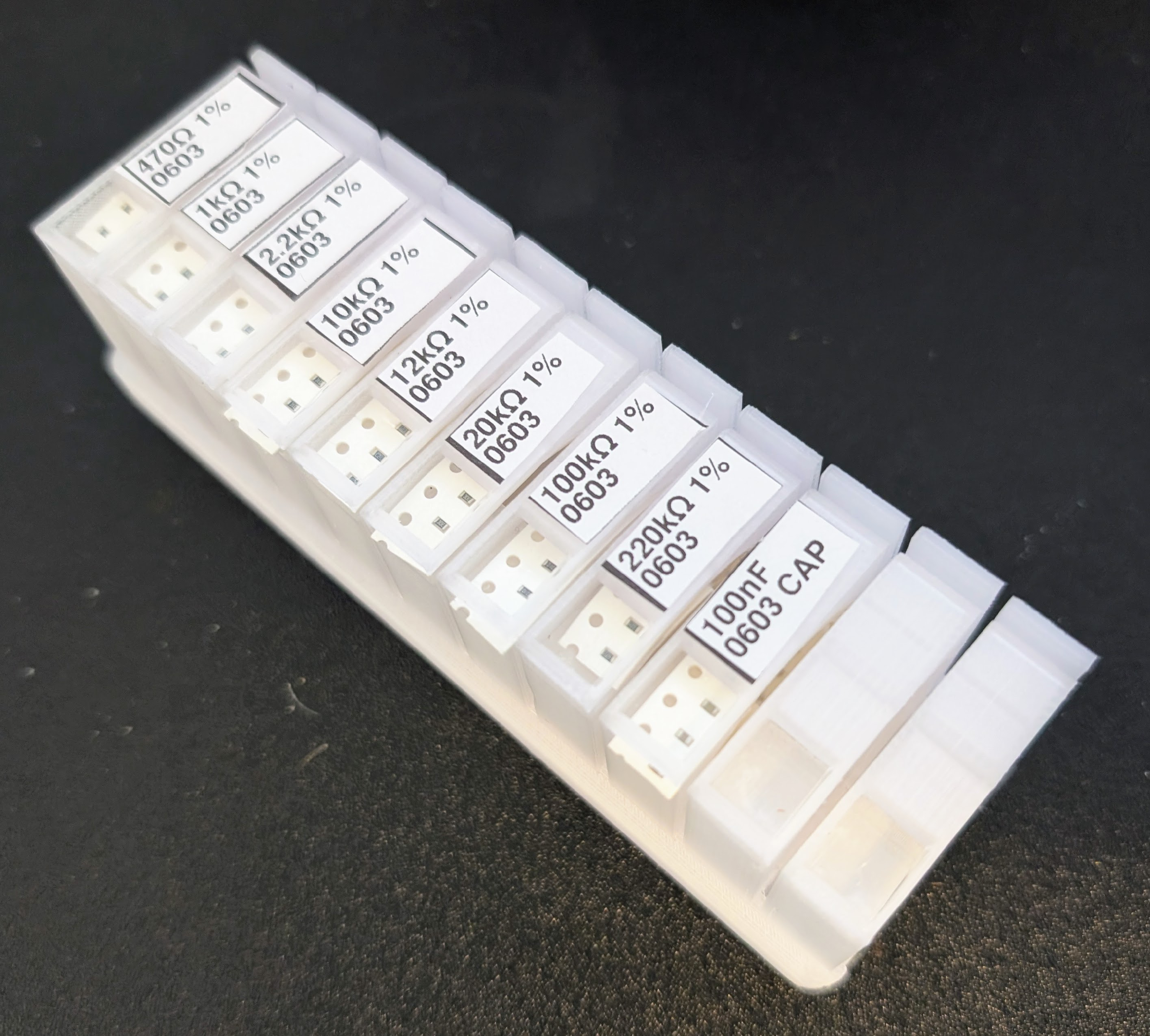
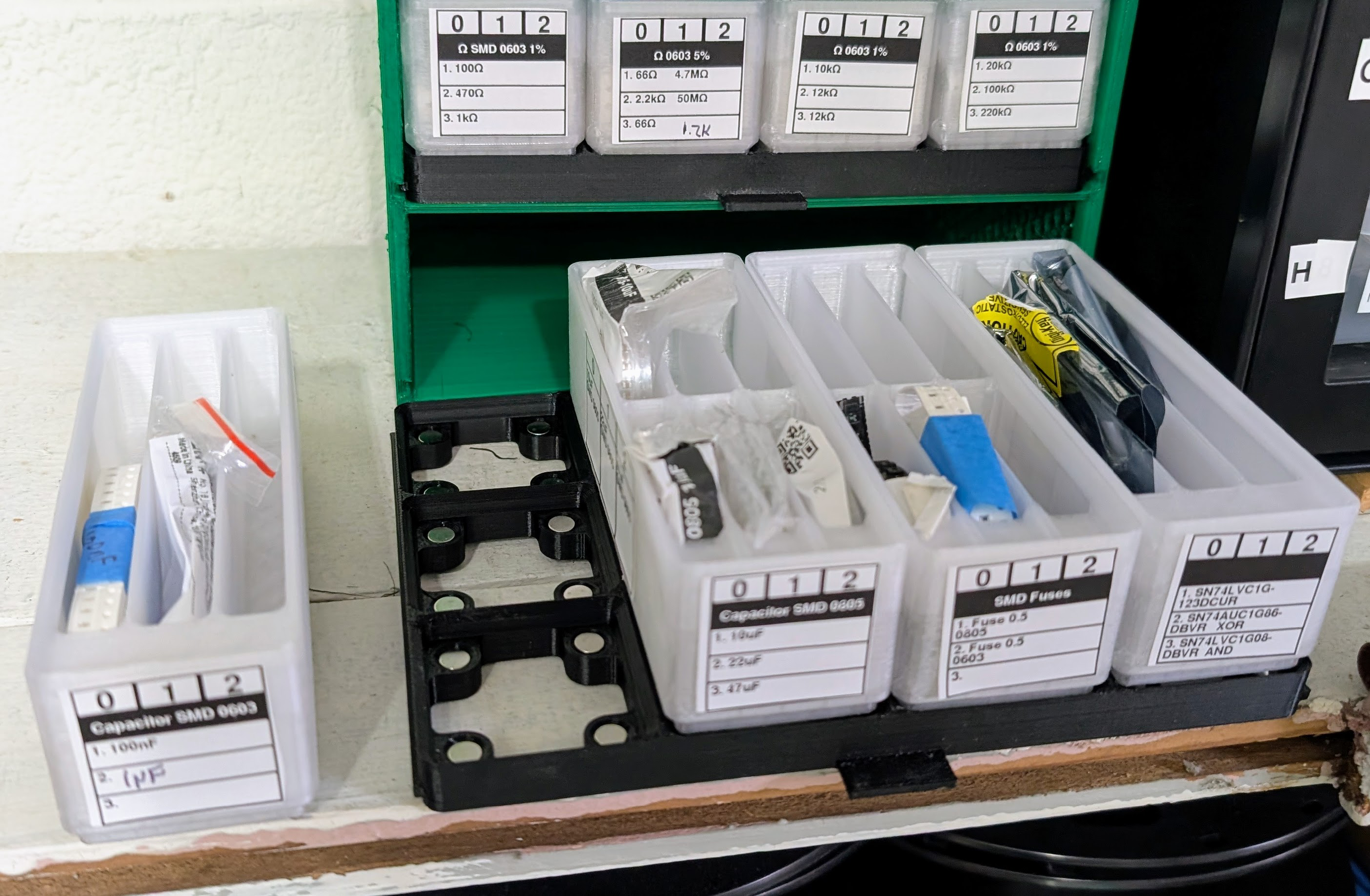
Gridfinity Pick-Bins for SMD Components
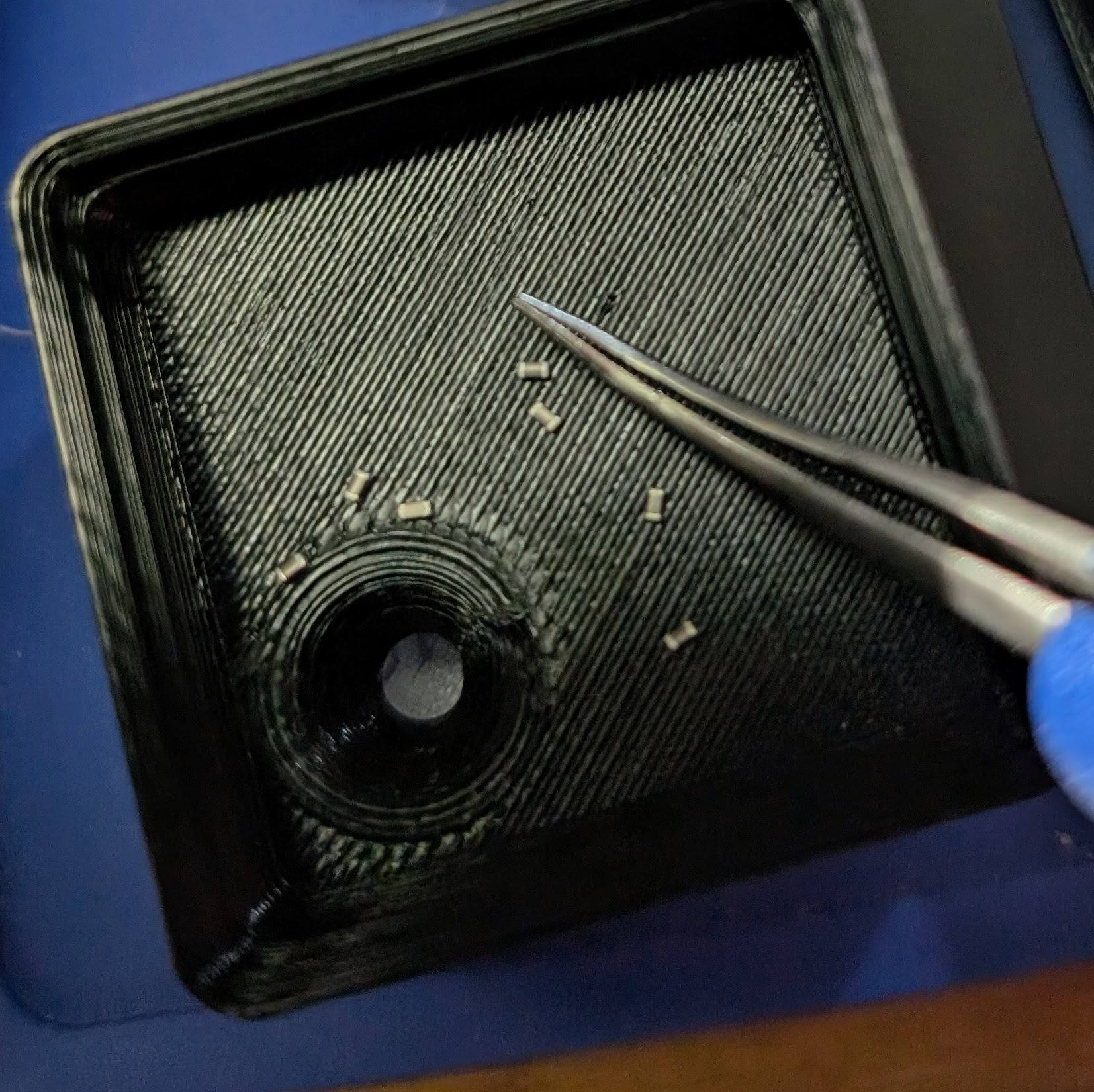
As mentioned before, it can be tricky to remove components from component-tape and not lose them. One obvious fix is to use some kind of bowl-shaped depression or funnel to corral components when removing them from tape, and a possibly smaller bowl-shaped depression to hold components when picking them up with tweezers.
Gridfinity2 is a system for building custom storage bins for small items. After playing with Gridfinity for organizing drawers, I realized it could also help me for managing SMD components. Using the OpenSCAD version of Gridfinity, I designed pick-bin trays for holding SMD components before and during assembly. I made a couple different versions of a “unit sized” Gridfinity tray with multiple shallow depressions for holding different kinds of SMD components. For very small components such as 0603 resistors, I find a tray divided into 2x2 pick-bins most useful.
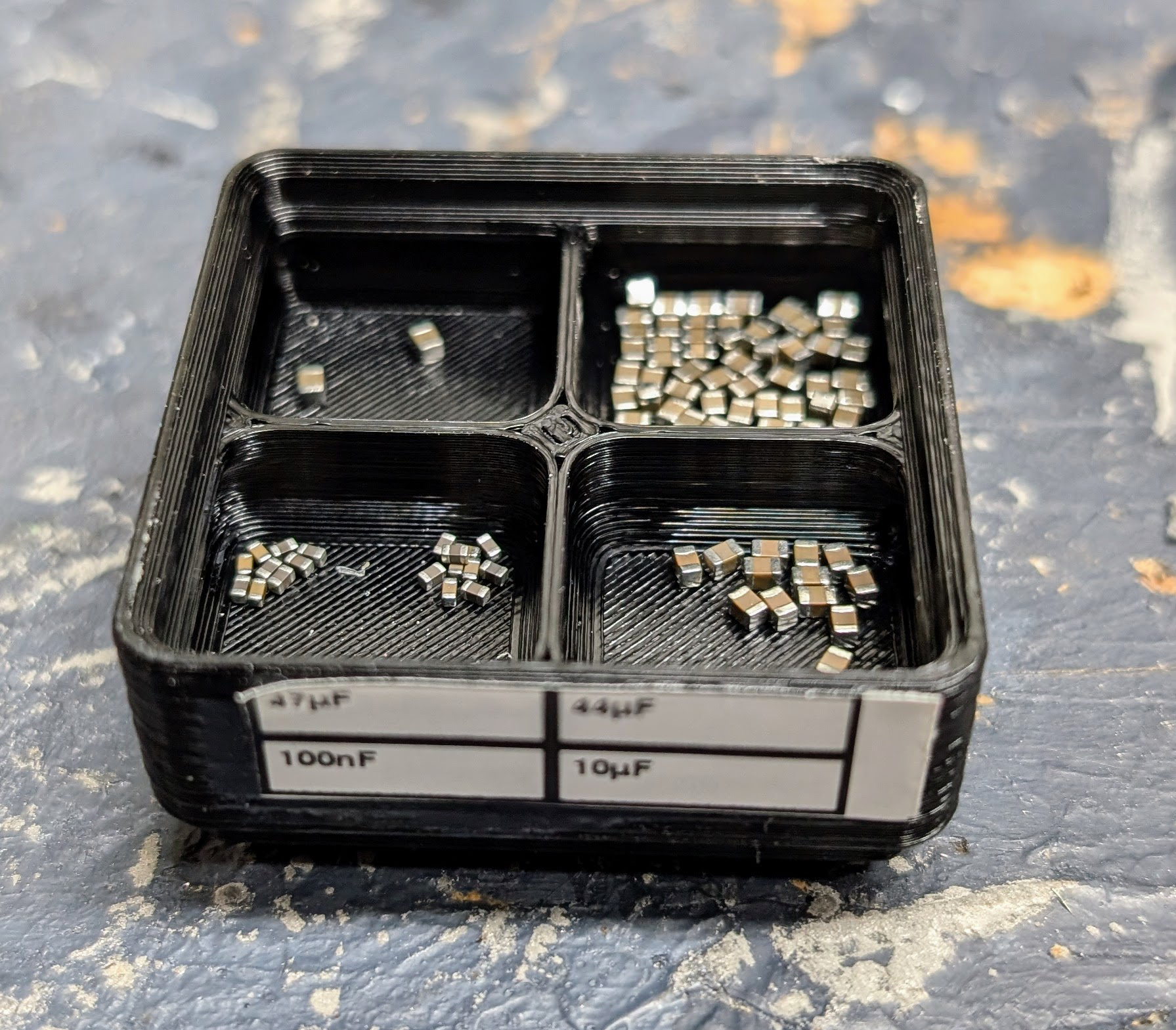
I wrote a Python-based web interface for generating custom labels for the front of the tray. I found that attaching labels to 3D-printed items does not work well. The cylindrical shape of extruded plastic dramatically limits the contact surface for adhesives. I painted some epoxy designed to coat 3D-printed objects on one side of the printed tray. This makes a smooth surface that works much better for applying printed labels.
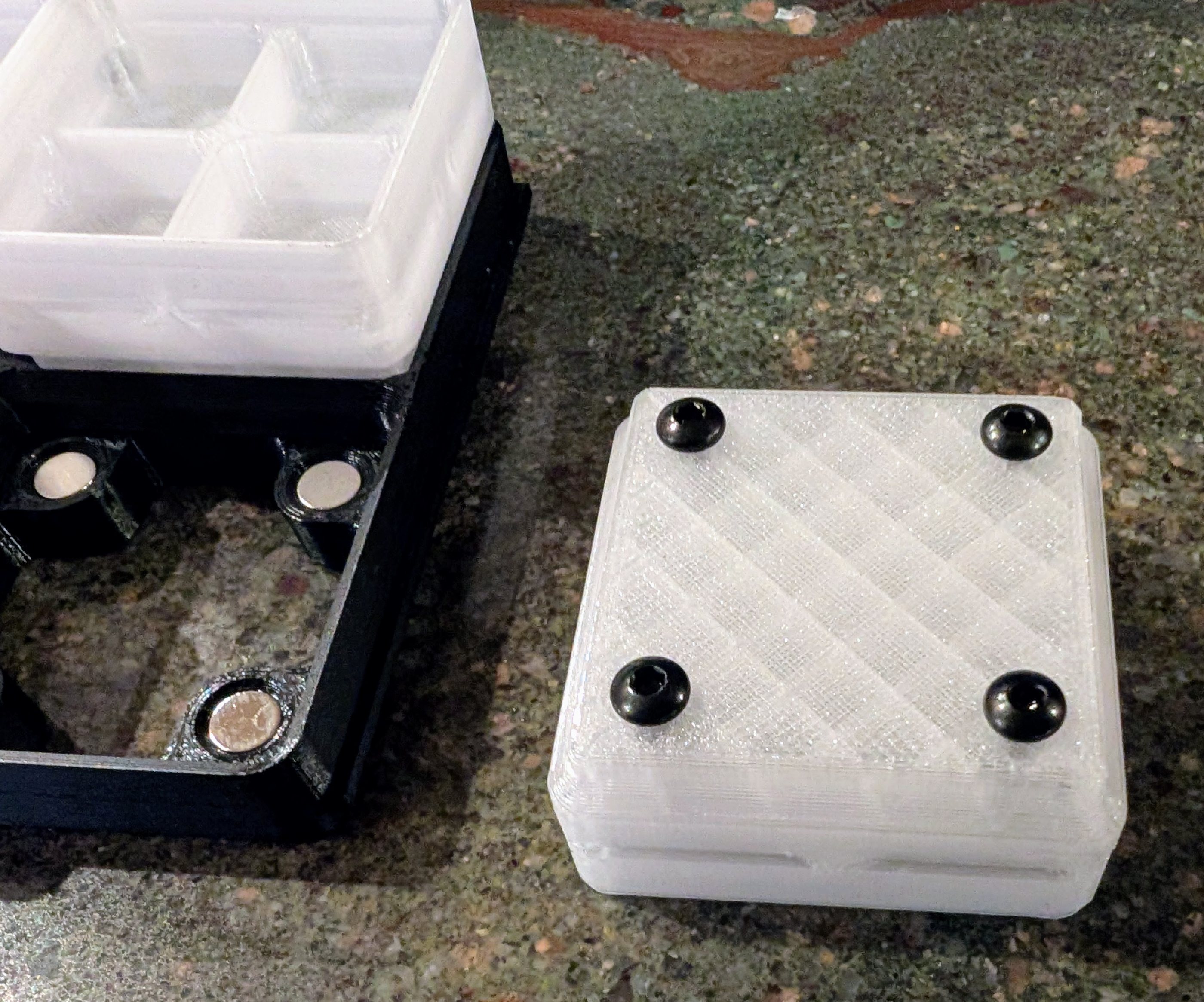
As will be shown later, M3 screws are screwed into the bottom of the pick-bin trays so they can be held in place within drawers with small magnets.
For larger components, a bin divided into two depressions is more appropriate than the 2x2 version.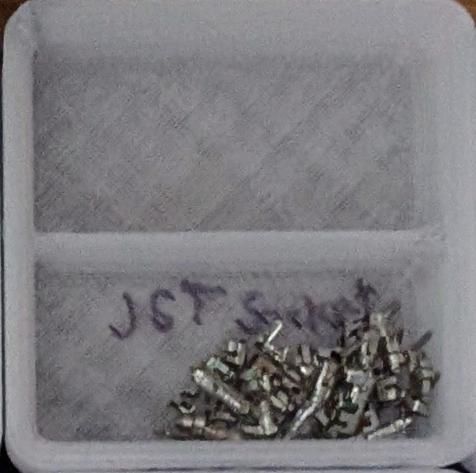
I also designed a small tray with a funnel-hole which would be at the center of one bin of a 2x2 pick-bin tray. Placing this funnel over a 2x2 tray makes it easy to remove a bunch of components from a tape and corral them into one of the 2x2 bins. Rotate the funnel with respect to the tray underneath to fill the other bins.
Before PCBA assembly, organize all the bins you will need, and make sure they have enough of each kind of component for populating the board or boards you are assembling.
Managing ESD Protection for 3D Printed Storage
Many components are sensitive to electrostatic discharge (ESD6). To protect against ESD I printed some of the pick-bin trays using ESD-safe printer filament: Fiberon PETG-ESD ( Amazon). This filament was recommended by colleagues at my workplace. It has carbon nanotubes which are conductive and prevent static charge build-up on the surface of printed items.
I’ve seen online that some people have concerns whether printing with carbon nanotubes might release fibers into the air that could cause damage to lungs, similar to the danger of asbestos fibers. It seems that the concern is not widespread, but I already print in a LAK enclosure in the basement (to keep the ambient air warm in the winter) and added a Bento-box air filter with a HEPA filter and activated carbon to run in the enclosure while the printer is using this filament.
Power to the filter is automated using Home Assistant7 and a Sonoff Basic relay running ESPHome8.
I’m not sure whether the filter actually helps. Maybe the fibers are long enough to get caught in the filter, but maybe they are just too small and pass through. This is completely outside any area of expertise for me. If you have relevant knowledge about the risk and reasonable methods of mitigation, please leave a note below!
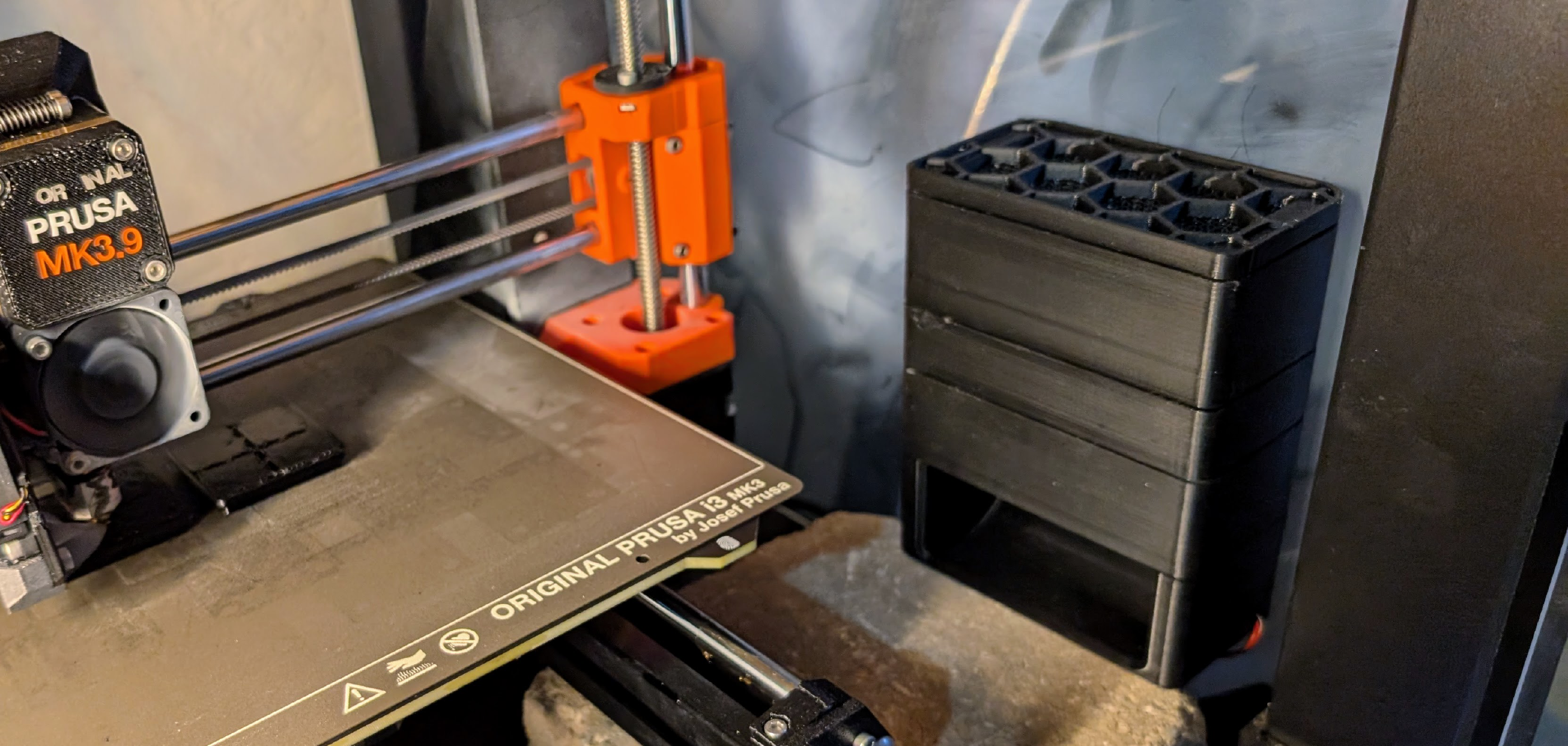
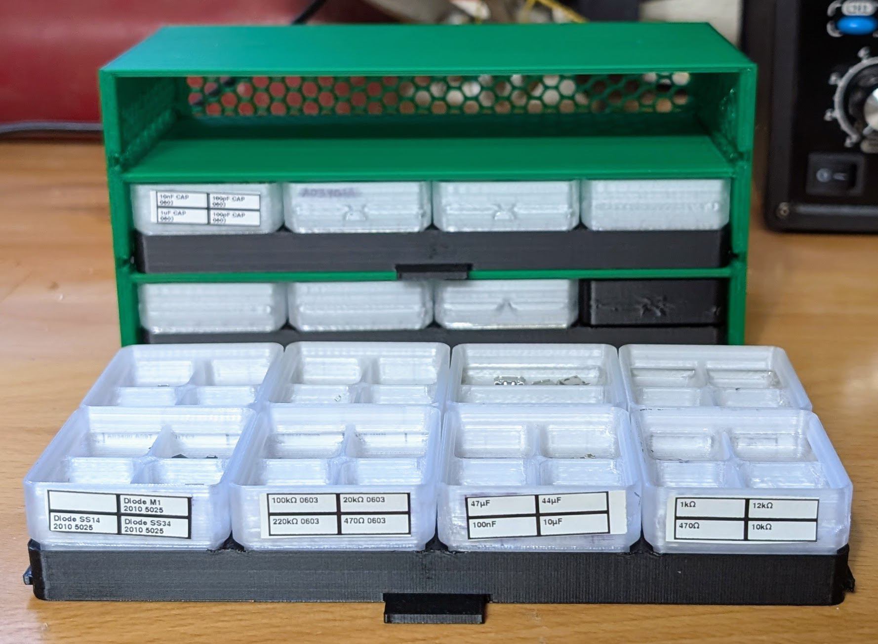
Custom 3D Printed SMD Storage Cabinet
A key motivating theme of Gridfinity is to keep everything visible in your workshop, not hidden away in drawers. But there are a wide variety of SMD components and workbench space is valuable, so I decided to try designing a cabinet for storing the pick-bin trays using less shelf and workbench surface area.
This way, after you are done assembling your boards you can put your pick-bins safely away where you can find them again next time.
A drawer is made of a Gridfinity base with a pull handle and simple guide rails on the sides.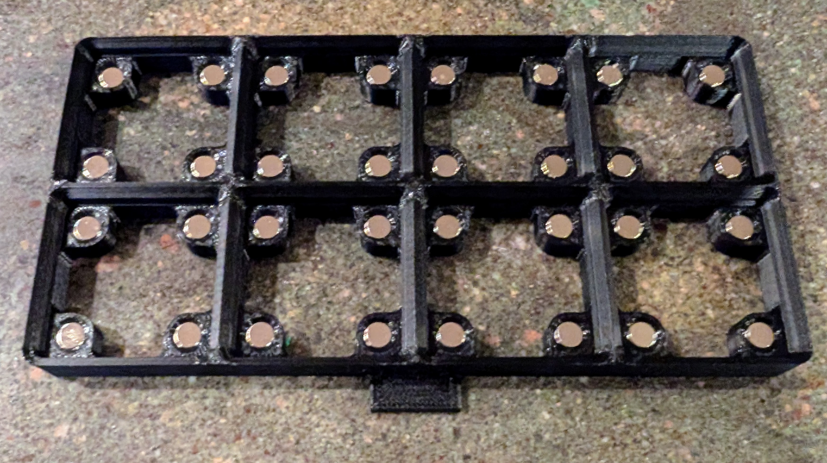
6x2mm magnets compression-fit into the drawer help hold the bin, which have M3 screws on their bottom side that line up with the magnets.
I designed a simple cabinet with space for the drawer with a set of SMD-pick bins on top of them.
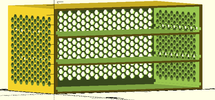
There is a slot in each drawer space in the cabinet for the rails along the drawer base to slide into.
The hex-pattern in the cabinet reduces material required to print it and makes the cabinet look a little less boring. The cabinet is 3D printed lying on its back so it requires no support material when printing.
Gridfinity Component Tape Dispensers
A co-worker recommended 3D-printable component tape organizers and dispensers as another way to deal with small components for assembly. Here is one which also works well with Gridfinity storage.
I found it is difficult to remove components from the tape from these dispensers using
tweezers, because there isn’t access space around the components.
However, if you buy a suction tool such as this one
Amazon
you can remove the small components from tape held in such a dispenser and place them
on your board.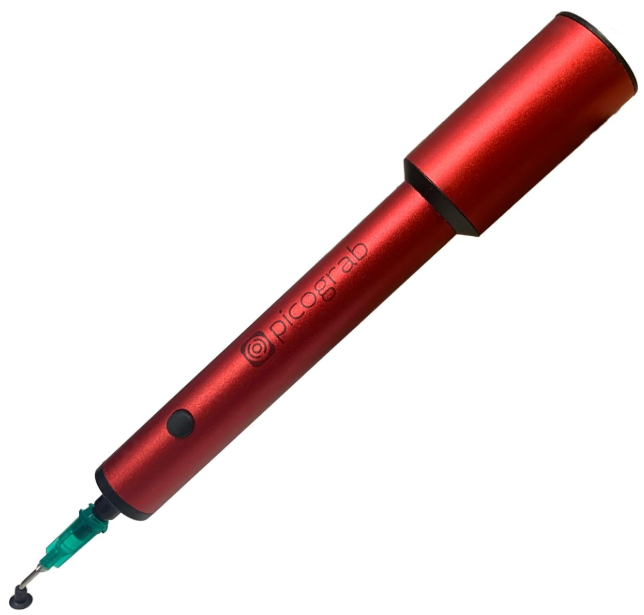
This is similar to how the tape is meant to be used with pick-and-place robots. It is a relatively expensive tool, so whether it is worth it depends on how much of this kind of assembly you will do.
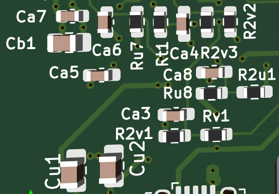
PCB Component Reference Designators for Easy Assembly
When picking components from the Gridfinity bins and placing them into place on the PCB, it helps not to need to look at the BOM or board diagram to determine component values. My boards have a bunch of 100nF capacitors, so I label these Ca1, Ca2, etc… I label 10uF capacitors Cb1, Cb2, etc… and so on. This way, I can quickly place a bunch of capacitors directly on the board without looking elsewhere. Similarly, I label the 10kΩ pull-up resistors as Ru1, Ru2, etc…, and 20kΩ as R2u1 and so on.
SMD Component Inventory Management
Getting a project done typically requires the use of a wide variety of random tools and components. So a big role of a workshop is to store a wide selection of things with some organization system such that you can quickly find things when you need them.
When I first started designing and building circuits, I found it was useful to buy kits with a
few items for a wide variety of components.
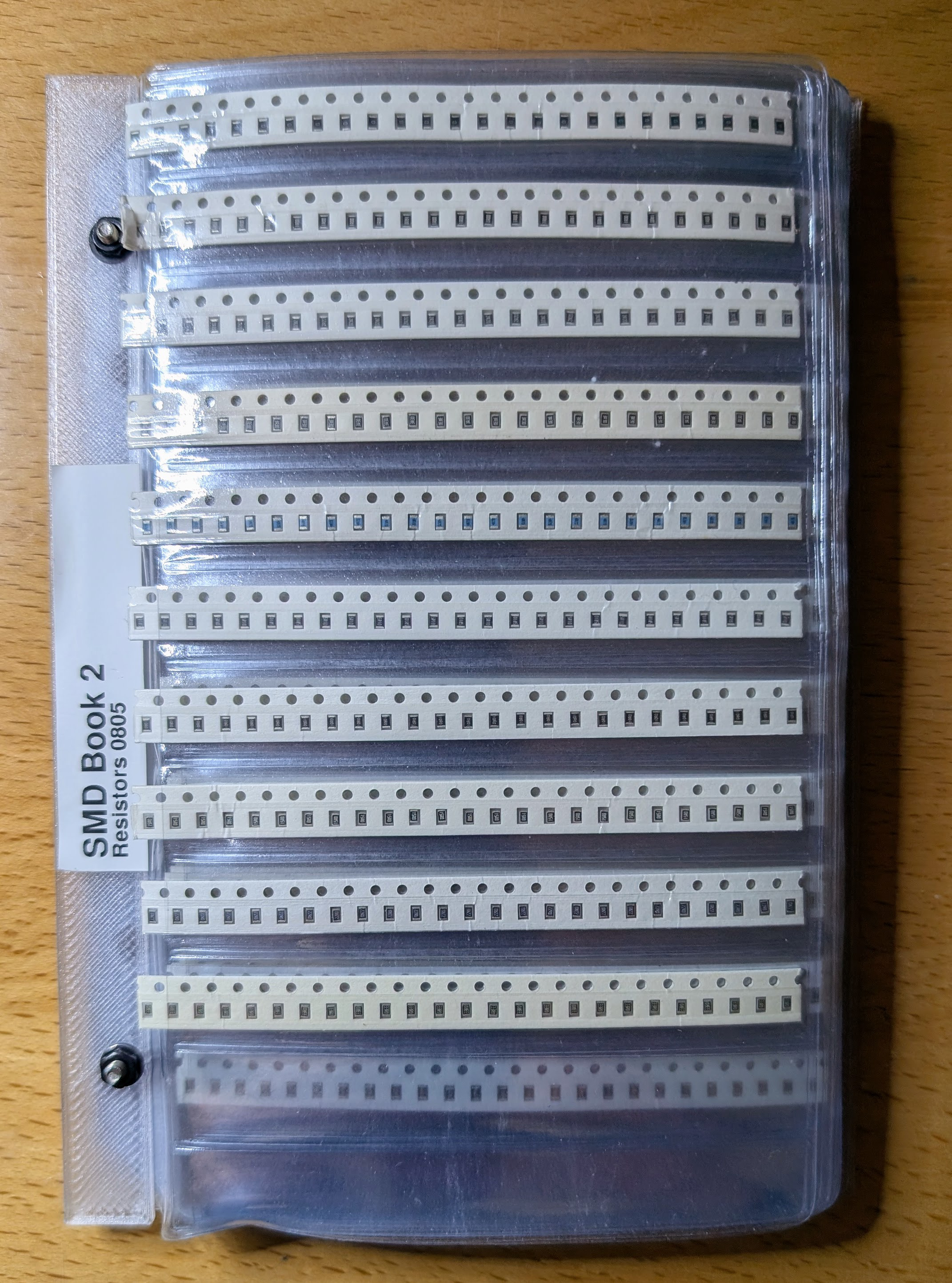
For example, I bought a book of 0603 resistors and a book of 0603 capacitors, and kits with
different kinds of Schottky diodes.
Component books are relatively expensive compared to the price of buying components themselves,
but give you a start with all component values you may need along with useful organization.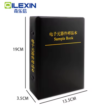
One alternative to buying component books is buying component kits, buying pages of component books, and making a DIY component book. After buying a couple books, I ordered a set of SMD component pages from AliExpress and 3D printed a very simple back cover and front plate to hold the pages together with some M3 screws. These made a component book which is functional, if a little awkward to remove sample tape sections from. The design can definitely be improved upon.
Especially for active components such as transistors, voltage regulators, and sensors, it is useful to have a database of available components in stock for use in new designs. I run Inventree, an open source inventory tracking system, on my homelab server for use in tracking available components, along with where these are are stored in my workshop. To get the specifications of purchased components into the database, I use Ki-n-Tree to query specifications from DigiKey and put them into the Inventree database. For components where I really want to be sure of specifications and performance, I purchase parts from DigiKey.
Bulk Storage Solutions for Electronic Components
For storing larger items like through-hole components, I found that standard storage cabinets
with small drawers work well.
Here is an Akro-Mils cabinet I use (
Amazon).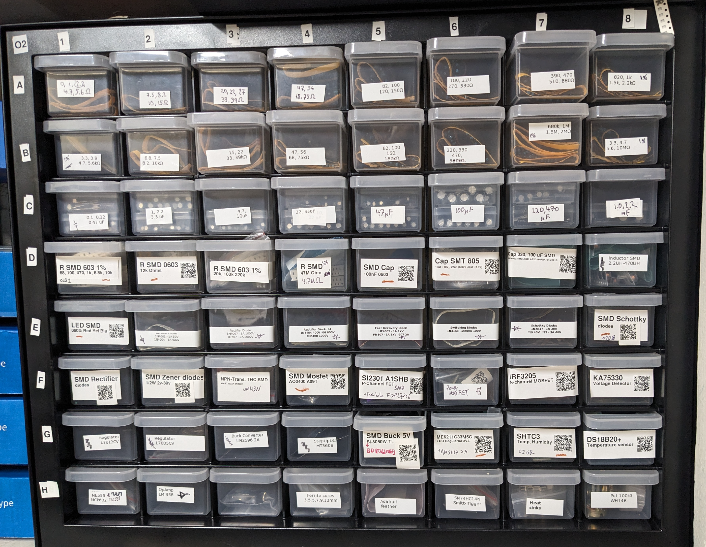
For storing bulk SMD components, however, I find this cabinet awkward. The drawers are too large for just a few components in a short tape, and not the most useful shape for large rolls of tape with many components.
I designed a set of larger bulk storage bins which would also fit on Gridfinity shelves in a simple cabinet.
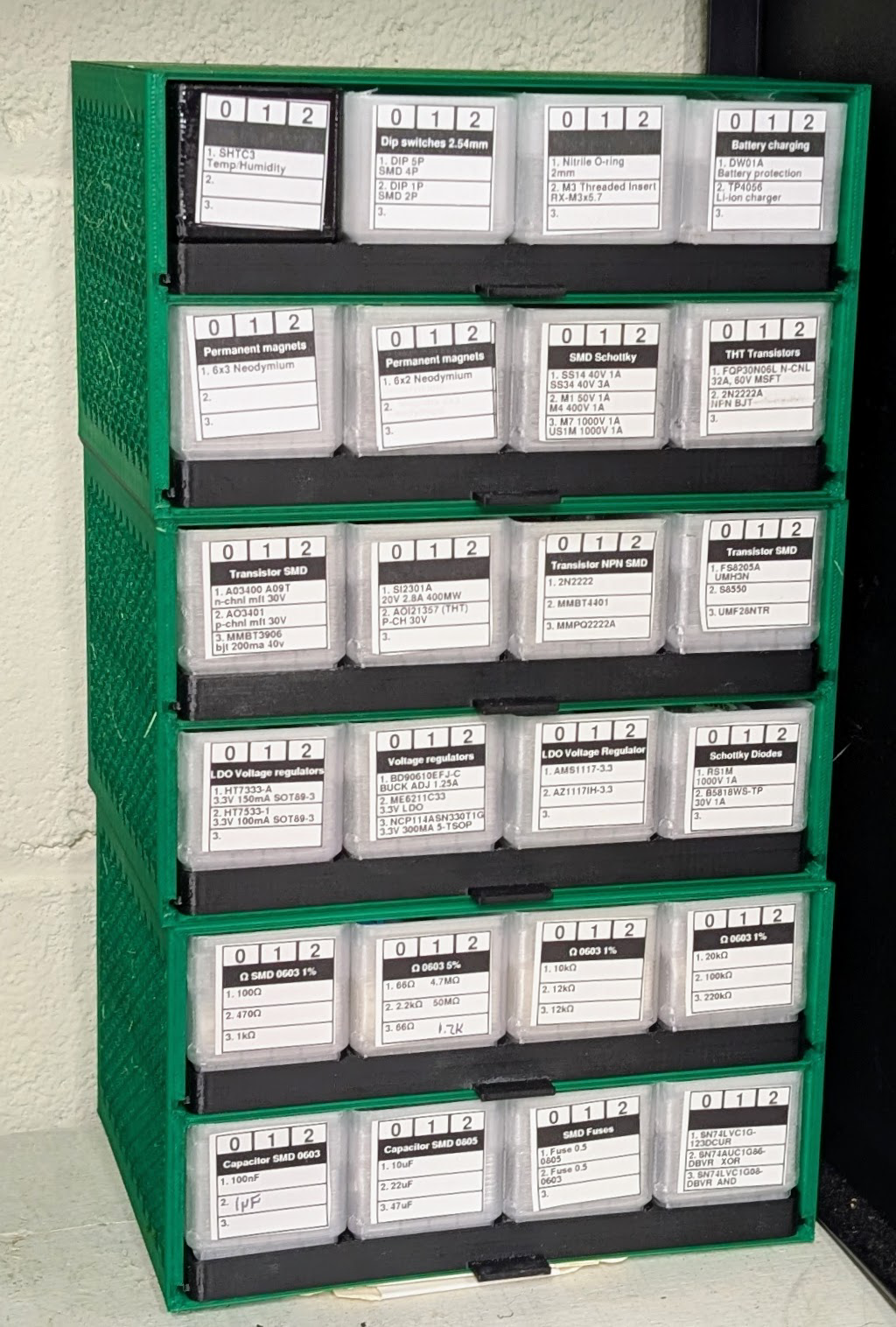
These bins can be subdivided in different ways for storing wider or thinner tapes, many short segments of tape, or just piles of larger individual components.
The design in in the GitHub repository, and also published at printables.com as SMT component bulk storage cabinet.
Custom Labeling System for Component Bins
For labeling the content of pick bins and bulk storage bins, I made a simple web interface with a Python backend that uses Pillow to generate .png files for labels, then sends these to a Brother RQL-810W- printer in the workshop. I will eventually publish this to Github but haven’t done this yet.
Conclusion
As mentioned before, this post is a grab-bag of designs and techniques from a self-taught hobbyist. Some of this might have been interesting or useful (to admittedly particular readers at least). I suspect more experienced engineers and hobbyists might find parts of it to be somewhat naive. Feel free to let me and any other readers know either way!
References
A printed circuit board (PCB) connects electrical components together to make an electical circuit. It is a laminated sandwich structure of conductive and insulated layers. ↩︎
Gridfinity is a modular storage system that is popular in the 3D-printing community. ↩︎ ↩︎
A surface mounted device (SMD) is an electrical component soldered directly onto the surface of a printed circuit board. This is in contrast to through-hole components where the electrical connections are wires that are soldered into holes through the circuit board. ↩︎
Bill of Materials (BOM). A list of components needed to assemble some end product. ↩︎
Electrostatic discharge (ESD) is a sudden and momentary flow of electric current between two differently-charged objects when brought close together or when the dielectric between them breaks down. ↩︎
Home Assistant is a popular Open Source home automation platform. It is the hub for my own smart home, and it is fun to work with. ↩︎
ESPHome is a system for building firmware for microcontrollers particularly for use in Home Automation applications. Specification for what the firmware should do is written in simple YAML files. ↩︎