Faster SMD Pick-and-Place: Tape Dispensers and Vacuum Tools
Posted on October 10, 2026 • Last modified on October 10, 2026 • 6 min read • 1,266 words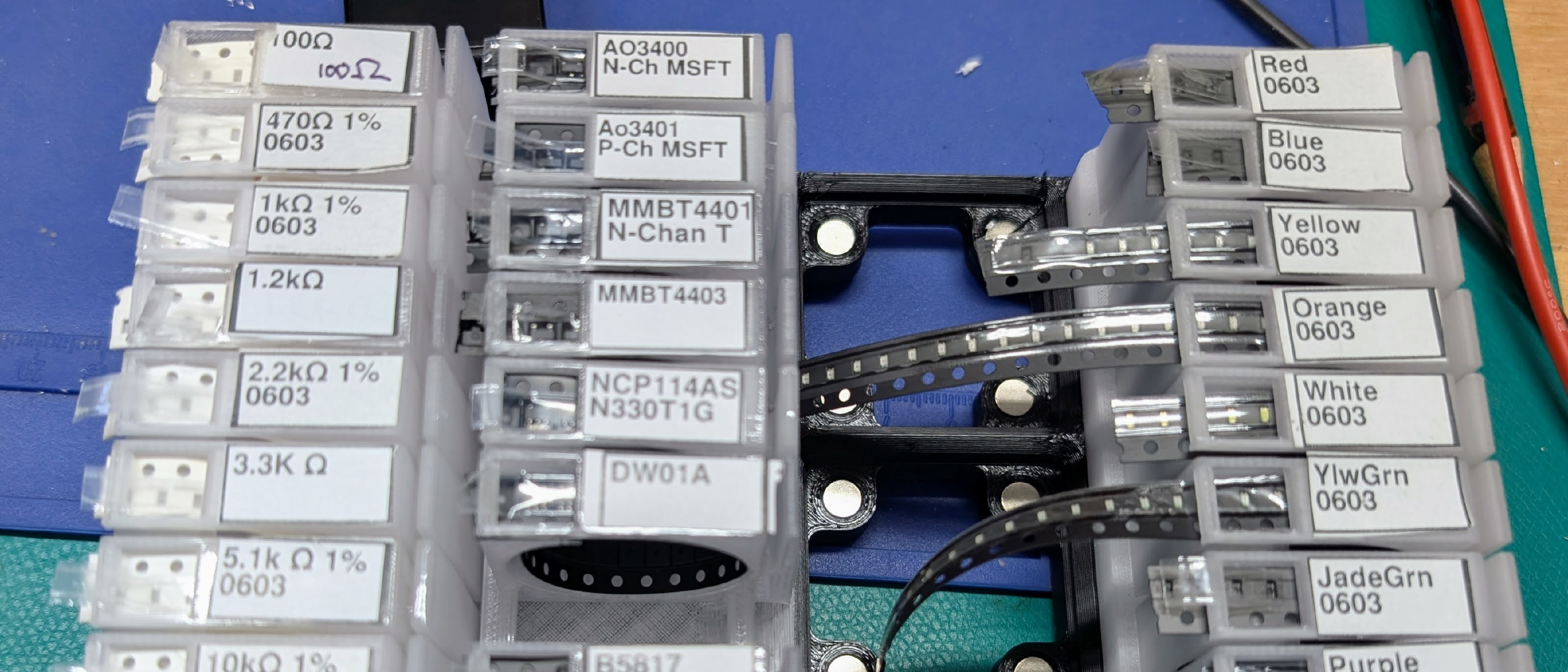
Introduction: Pick Bins Can Be Slow
In DIY SMD PCB Assembly , I described my setup for hand-assembling printed circuit boards (PCBs1) with surface-mount devices (SMD2). That workflow centered around 3D-printed Gridfinity3 bins for storing cut tape and loose parts, custom stencils4 for applying solder paste, and a modified reflow oven5. Later, in Improved PCB Stencil Alignment , I refined the solder paste application step using a 3D-printed alignment fixture.
Once solder paste is deposited onto the PCB, the most time-consuming phase of assembly begins: populating dozens of components onto their pasted pads. Sorting components into open pick-bins was faster than wrestling with cut tape at the bench. However, picking loose parts with fine-tipped tweezers introduced several frustrating failure modes:
- Surface-mount passives (especially 0603 and 0805 packages) frequently land upside-down in bins, requiring manual nudging to flip them over before picking.
- Polarized components—such as indicator LEDs, diodes, and SOT-236 transistors—tumble into random rotations. Identifying microscopic cathode markings or pin-1 dots under the microscope for every individual part slows down assembly.
- Applying slightly uneven lateral pressure with tweezers can launch tiny components across the workshop, never to be found again.
- If a loose component bin is accidentally bumped or dropped, sorting through a mixture of LEDs of different colors or unmarked ceramic capacitors is nearly impossible.
The Vacuum Suction Pen
A work colleague suggested placing components directly from cut tape rather than sorting them into loose pick-bins. To try this workflow, I ordered a cordless electric vacuum suction pen and found tape-based component dispensers to print for use with my bulk component cabinets.
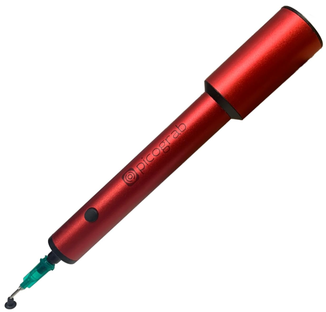
The pen features an internal micro-vacuum pump powered by a lithium battery that recharges via USB-C. It includes several angled nozzles fitted with interchangeable silicone suction cups of varying diameters, allowing it to handle everything from 0603 passives up to SOT-23 transistors and small ICs. While the electric vacuum pen seemed relatively expensive compared to a pair of tweezers, the dramatic speed improvement easily justified the cost.
Key advantages over tweezers include:
- Eliminating component launch: Because the suction cup grips the flat top surface of the component rather than applying lateral clamping force, there is zero spring tension waiting to fling parts across the workbench.
- Direct vertical placement: The tool allows you to lower a part straight down into the solder paste without disturbing adjacent deposits or bridging fine-pitch pads.
- Preserved orientation: Components stored in tape are already right-side-up, and picking from above maintains their alignment from tape pocket to PCB.
Modular Tape-Based Dispensers
The second half of the upgrade involved rethinking how components are stored and presented at the workbench. Instead of dumping components into open bins, I began loading cut tape strips directly into 3D-printed tape dispensers.
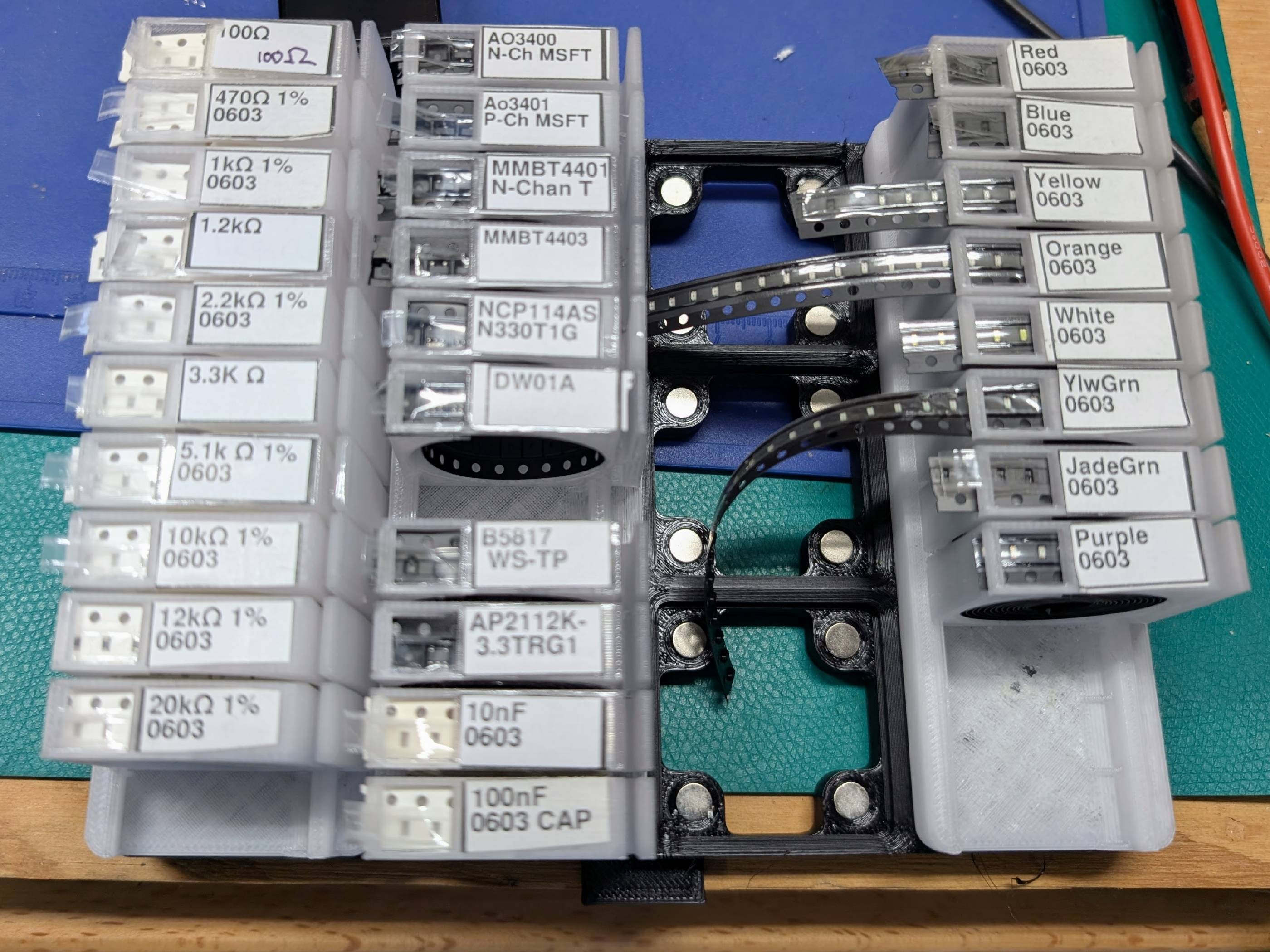
In the image above, the tape dispensers snap into Gridfinity holder bases. These bases in turn sit in a Gridfinity drawer that slides into one of my bulk storage cabinets.
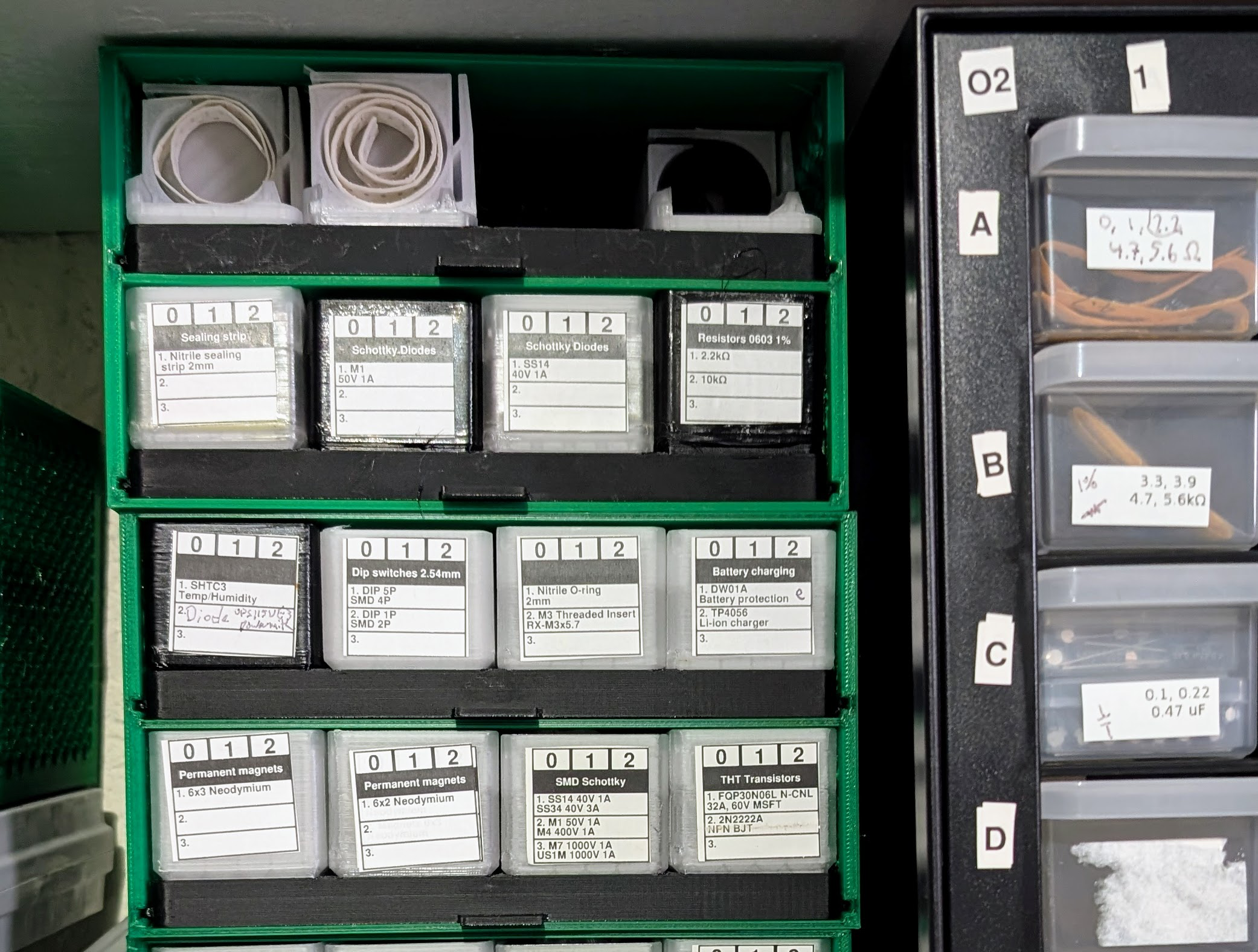
While tape dispensers are commonly associated with high-turnover resistors and capacitors, they are equally valuable for discrete active and polarized components such as status LEDs, switching diodes, and small transistors.
This setup provides several practical advantages:
- Predetermined pin-1 and polarity orientation: In loose bins, identifying cathode bands or transistor pinouts requires constant visual verification. In carrier tape, components are factory-packaged in a fixed, standardized orientation relative to the sprocket holes (per EIA-4817). Advancing the tape presents each diode, LED, or transistor in the exact same orientation every time, drastically speeding pick-and-place.
- Controlled exposure: The dispenser mechanism only peels back the clear cover film for the single component about to be picked. If a dispenser rack is bumped, dropped, or knocked off the table, only the single exposed part is lost rather than an entire drawer of loose inventory.
- High storage density: A single drawer of dispensers holds dozens of tape strips, which in turn can store hundreds of components. The resulting storage density is substantially higher than open bins.
- Rapid bench setup: High-turnover parts—such as 0.1 µF bypass capacitors, 10 kΩ pull-ups, 5.1 kΩ USB-C resistors, status LEDs, and common transistors—stay permanently loaded in modular racks. Preparing the bench for a batch assembly session simply requires pulling the dispenser shelf from the storage cabinet and placing it next to the microscope.
Combined Workflow
Combining the tape dispensers with the vacuum suction pen creates a smooth, rhythmic assembly process:
- The PCB is printed with solder paste using the 3D-printed alignment fixture.
- The board is secured under the microscope.
- The dispenser shelf is placed directly adjacent to the board.
- With one hand advancing the tape strips, the other hand uses the vacuum pen to pick each component and place it directly onto the pasted pads.
In practice, this combination is noticeably faster, more ergonomic, and far less error-prone than picking loose parts with tweezers. Any high-turnover surface-mount components in my workshop—whether passives, transistors, or LEDs—are now permanently organized in this dispenser system.
Stencil Fixture with Support Frame
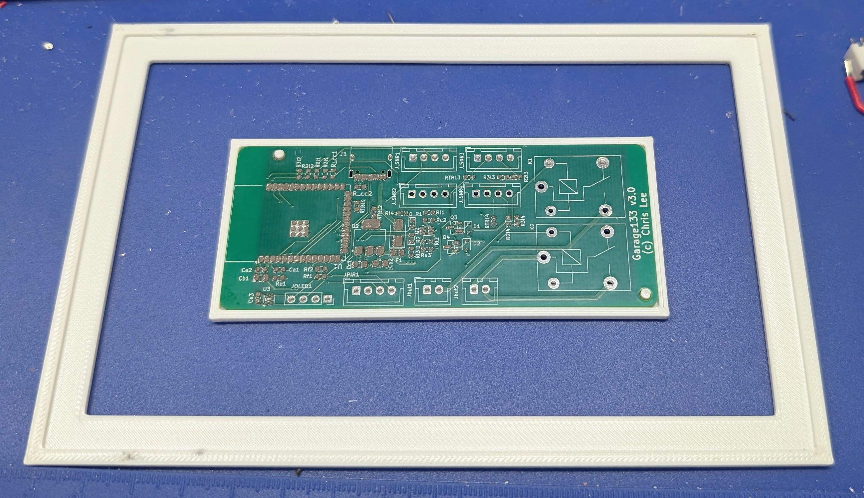
I have also made a small refinement to my 3D-printed fixture for aligning PCB stencils . Frameless stainless steel stencils from board vendors such as blog sponsor PCBWay are typically much larger than the PCB itself (such as a 150×150 mm stencil for an 80×50 mm board). Unless I am assembling a large batch of identical boards, it is not worthwhile to print a solid fixture that spans the entire stencil area. This would consume excessive filament and hours of print time. However, if the fixture only supports the PCB in the center, the wide unsupported metal borders droop and flex under the pressure of the putty knife, causing the solder paste to smear.
To solve this, I now print a reusable outer frame that supports the perimeter of standard stencil sheet sizes. A much smaller, board-specific insert sits inside the frame to hold the PCB flush and align the registration pins. This modular combination keeps the metal stencil completely flat across its entire surface during paste application while keeping 3D-print times for new board designs short.
References
-
A printed circuit board (PCB) connects electrical components together to make an electrical circuit. It is a laminated sandwich structure of conductive and insulated layers. ↩︎
-
A surface-mounted device (SMD) is an electrical component soldered directly onto the surface of a printed circuit board. This is in contrast to through-hole components where the electrical connections are wires that are soldered into holes through the circuit board. ↩︎
-
Gridfinity is a modular storage system that is popular in the 3D-printing community. ↩︎
-
A solder paste stencil is a laser-cut foil (typically stainless steel or polyimide) with apertures matching surface-mount PCB pad layouts, used to accurately deposit solder paste onto pads prior to component placement. ↩︎
-
Reflow oven : an oven with precise thermal profiling used for reflow soldering of surface-mount electronic components to printed circuit boards. ↩︎
-
SOT-23 (Small Outline Transistor): a compact surface-mount plastic package with gull-wing leads commonly used for discrete transistors and diodes. ↩︎
-
EIA-481 : an industry standard published by the Electronic Industries Alliance defining the dimensions and specifications for embossed and punched carrier taping of surface-mount components for automated handling. ↩︎